About PCB Design And Project Development
HBeonLabs Technologies offers comprehensivePCB Design and Project Development Services, providing complete electronic product development solutions from initial concept to a fully functional, production-ready prototype. With deep expertise in embedded systems, power electronics, IoT, and automation, we help startups, enterprises, and innovators turn ideas into real, manufacturable hardware products.
OurPCB design servicesbegin with detailedschematic capture, followed bymulti-layer PCB layoutusing industry-standard tools such asAltium Designer, KiCad, Eagle, andOrCAD. We optimize every design forsignal integrity,thermal efficiency,EMI/EMC compliance, andDesign for Manufacturability (DFM). Whether its a compact IoT sensor node, a complex industrial controller, or a high-frequency RF board, we tailor the design to your exact requirements.
Beyond PCB design, HBeonLabs offers fullproject developmentsupport, includingmicrocontroller programming,firmware development,power supply design,sensor integration,wireless communication (LoRa, GSM, Wi-Fi, BLE), andmechanical enclosure design. Our team takes care ofcomponent sourcing,prototype fabrication,assembly, andfunctional testing, ensuring that every project meets performance, quality, and cost benchmarks.
We specialize in deliveringend-to-end solutionsfor applications such as:
-
IoT-based monitoring and control systems
-
Industrial automation and process control
-
Solar pump controllers and smart energy devices
-
RFID-based access and attendance systems
-
Smart agriculture, healthcare, and wearable electronics
With rapid prototyping capabilities and an agile development approach, HBeonLabs Technologies helps reduce time-to-market and technical risk making us a trusted partner forinnovation, product engineering, and scalable electronics development.
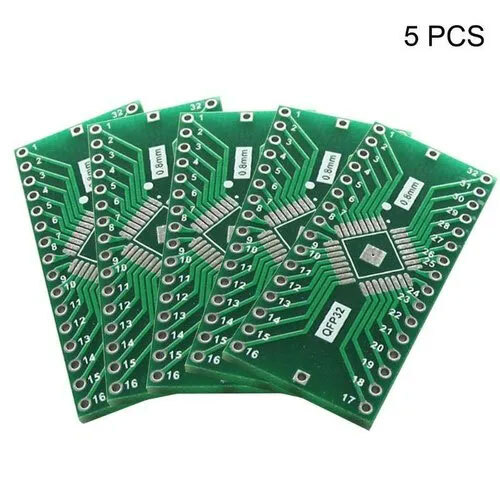
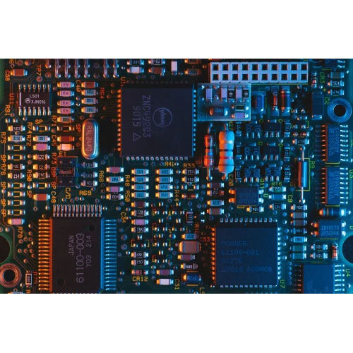
Comprehensive PCB Design SolutionsLeveraging top-tier design tools, we deliver robust PCB layouts compatible with embedded and industrial electronics. Our experts handle every element from schematic capture to component placement, ensuring reliable performance and manufacturability. Rigorous testing and validation guarantee each board meets exacting standards.
Rapid Prototyping and High-Precision ManufacturingWith flexible prototype lead times of 510 working days, we provide quick turnaround for urgent projects. Our assembly process employs high-precision SMD and through-hole techniques, resulting in consistently high component placement accuracy. All boards undergo thorough quality assurance and functional tests.
Flexible Customization and Project SupportClients benefit from extensive customization options, including design modifications, reverse engineering, and tailored prototyping. Transparent documentation and ongoing communication enable smooth collaboration. We provide support throughout India, handling projects both remotely and onsite as required.
FAQs of PCB Design And Project Development:
Q: How does the PCB Design and Project Development process work?
A: Our process begins with a requirements consultation, followed by schematic design using Altium Designer, Eagle, OrCAD, or Proteus. We create detailed layouts, perform prototype fabrication, assemble using high-precision SMD and through-hole techniques, then conduct rigorous testing and deliver complete documentation.
Q: What PCB layer configurations can you handle?
A: We design and develop single, double, and multi-layer PCB boards, allowing for a range of complexities tailored to specific project needs and performance criteria.
Q: When can I expect prototype delivery after placing my order?
A: Prototypes are fabricated and delivered within 510 working days, ensuring a swift response to your development timeline and project milestones.
Q: Where do you provide your PCB design services?
A: Our PCB design and development services are available throughout India. We support both remote (online) and onsite (offline) engagement as per the requirements of your project.
Q: What technical documentation will I receive with my PCB project?
A: You will receive comprehensive documentation including schematics, Gerber files, BOM (Excel format), and detailed testing reports to support manufacturing, assembly, and subsequent maintenance.
Q: How precise is the component placement on the PCBs?
A: We ensure high placement accuracy by utilizing advanced SMD and through-hole techniques, guaranteeing reliable electrical connections and consistent quality in assembled boards.
Q: What benefits does custom prototyping and testing provide?
A: Custom prototyping and thorough testingincluding power-on and functional validationoffer assurance that your final PCB meets application-specific requirements, minimizes risks, and streamlines the integration into your industrial or embedded system projects.


 Send Inquiry