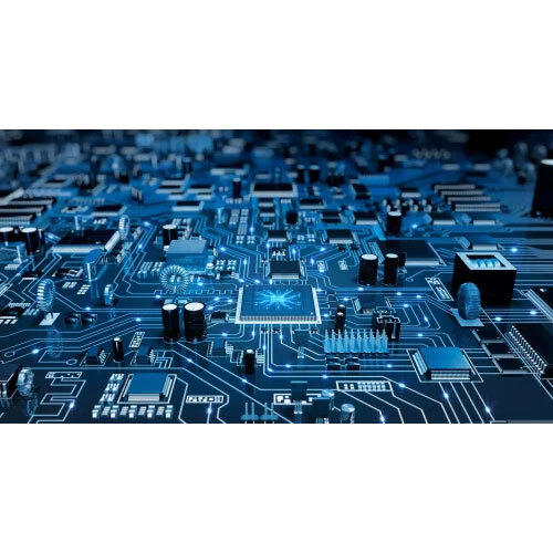
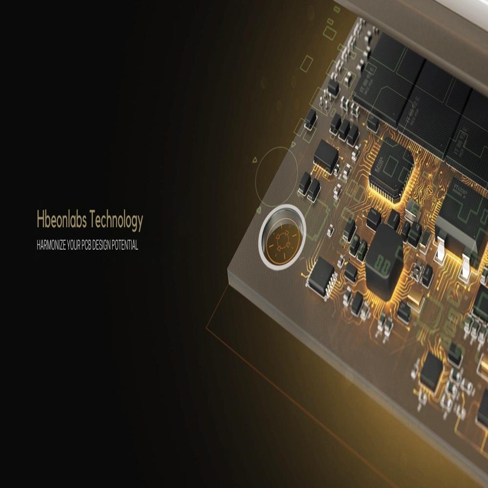
About PCB Design
HBeonLabs Technologies offers comprehensive PCB Design and Project Development Services, providing complete electronic product development solutions from initial concept to a fully functional, production-ready prototype. With deep expertise in embedded systems, power electronics, IoT, and automation, we help startups, enterprises, and innovators turn ideas into real, manufacturable hardware products.
Our PCB design services begin with detailed schematic capture, followed by multi-layer PCB layout using industry-standard tools such as Altium Designer, KiCad, Eagle, and OrCAD. We optimize every design for signal integrity, thermal efficiency, EMI/EMC compliance, and Design for Manufacturability (DFM). Whether its a compact IoT sensor node, a complex industrial controller, or a high-frequency RF board, we tailor the design to your exact requirements.
Beyond PCB design, HBeonLabs offers full project development support, including microcontroller programming, firmware development, power supply design, sensor integration, wireless communication (LoRa, GSM, Wi-Fi, BLE), and mechanical enclosure design. Our team takes care of component sourcing, prototype fabrication, assembly, and functional testing, ensuring that every project meets performance, quality, and cost benchmarks.
We specialize in delivering end-to-end solutions for applications such as:
-
IoT-based monitoring and control systems
-
Industrial automation and process control
-
Solar pump controllers and smart energy devices
-
RFID-based access and attendance systems
-
Smart agriculture, healthcare, and wearable electronics
With rapid prototyping capabilities and an agile development approach, HBeonLabs Technologies helps reduce time-to-market and technical risk making us a trusted partner for innovation, product engineering, and scalable electronics development.
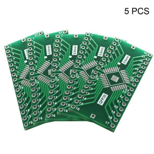
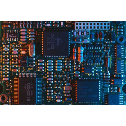
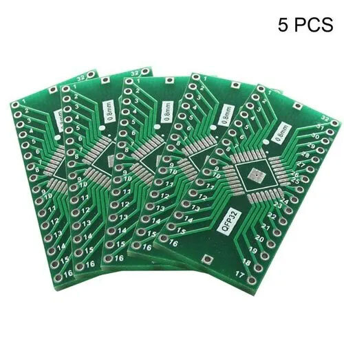
Precision Engineering for Demanding ApplicationsDesigned for reliability and high performance, our PCBs are equipped with state-of-the-art features such as advanced surface finishes, tight tolerances, and controlled impedance. Suitable for applications in consumer electronics, industry, automotive, and healthcare, we ensure each board is manufactured to exacting standards using both manual and automated operations.
Versatile and Customizable PCB SolutionsChoose from a comprehensive range of options, including green solder mask, white silkscreen, and multiple copper and board thicknesses. With support for file formats like Gerber and ODB++, and testing methods like Flying Probe and E-Test, our PCBs fit diverse development needs and offer seamless compatibility with your design processes.
FAQs of PCB Design:
Q: How does impedance control in your PCBs benefit specialized applications?
A: Impedance control ensures consistent signal integrity, which is critical for high-speed or sensitive circuits in automotive, medical, and industrial electronics. It helps prevent data loss and interference, ensuring your devices operate reliably under various conditions.
Q: What surface finishes are available and how do they impact performance?
A: We offer gold plating (ENIG), lead-free HASL, and OSP finishes. Gold plating provides excellent corrosion resistance and durability, making it suitable for high-reliability applications, while HASL and OSP offer cost-effective choices for general use. All options comply with RoHS standards.
Q: When should I select multilayer PCBs instead of single or double layers?
A: Multilayer PCBs are recommended when your design requires higher circuit density, complex routing, or enhanced performance, typically used in advanced consumer electronics, automotive controls, and medical devices. Single and double-layer boards suffice for simpler applications.
Q: Where are your PCBs manufactured and what is your production capacity?
A: Our PCBs are manufactured in India, utilizing advanced facilities with both automatic and manual processes. We maintain a monthly production capacity of 5,000 square meters to efficiently cater to large-scale as well as specialized orders.
Q: How do I submit my PCB design files for manufacturing?
A: You can submit your PCB designs in Gerber or ODB++ formats. These are industry-standard file types, ensuring your layout and specifications are accurately interpreted by our manufacturing systems for optimal results.
Q: What testing methods are used to ensure quality and reliability?
A: Each PCB undergoes Flying Probe and E-Test procedures, which check for electrical continuity and shorts across the board. These methods ensure every board meets quality standards before leaving our facility.
Q: What are the key usage benefits of your gold-plated, lead-free PCBs?
A: Our PCBs offer superior durability, environmental compliance, and excellent electrical performance. The gold-plated and lead-free options promote longevity and reliability, crucial for sensitive and mission-critical electronic equipment.


 Send Inquiry