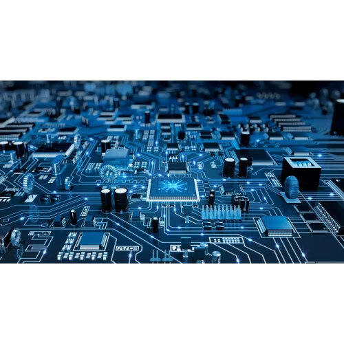
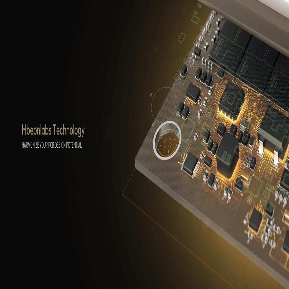
About PCB design and making facility
HBeonLabs Technologies offers comprehensivePCB Design and Project Development Services, providing complete electronic product development solutions from initial concept to a fully functional, production-ready prototype. With deep expertise in embedded systems, power electronics, IoT, and automation, we help startups, enterprises, and innovators turn ideas into real, manufacturable hardware products.
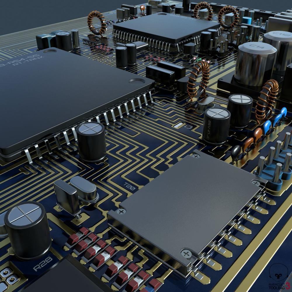
OurPCB design servicesbegin with detailedschematic capture, followed bymulti-layer PCB layoutusing industry-standard tools such asAltium Designer, KiCad, Eagle, andOrCAD. We optimize every design forsignal integrity,thermal efficiency,EMI/EMC compliance, andDesign for Manufacturability (DFM). Whether its a compact IoT sensor node, a complex industrial controller, or a high-frequency RF board, we tailor the design to your exact requirements.
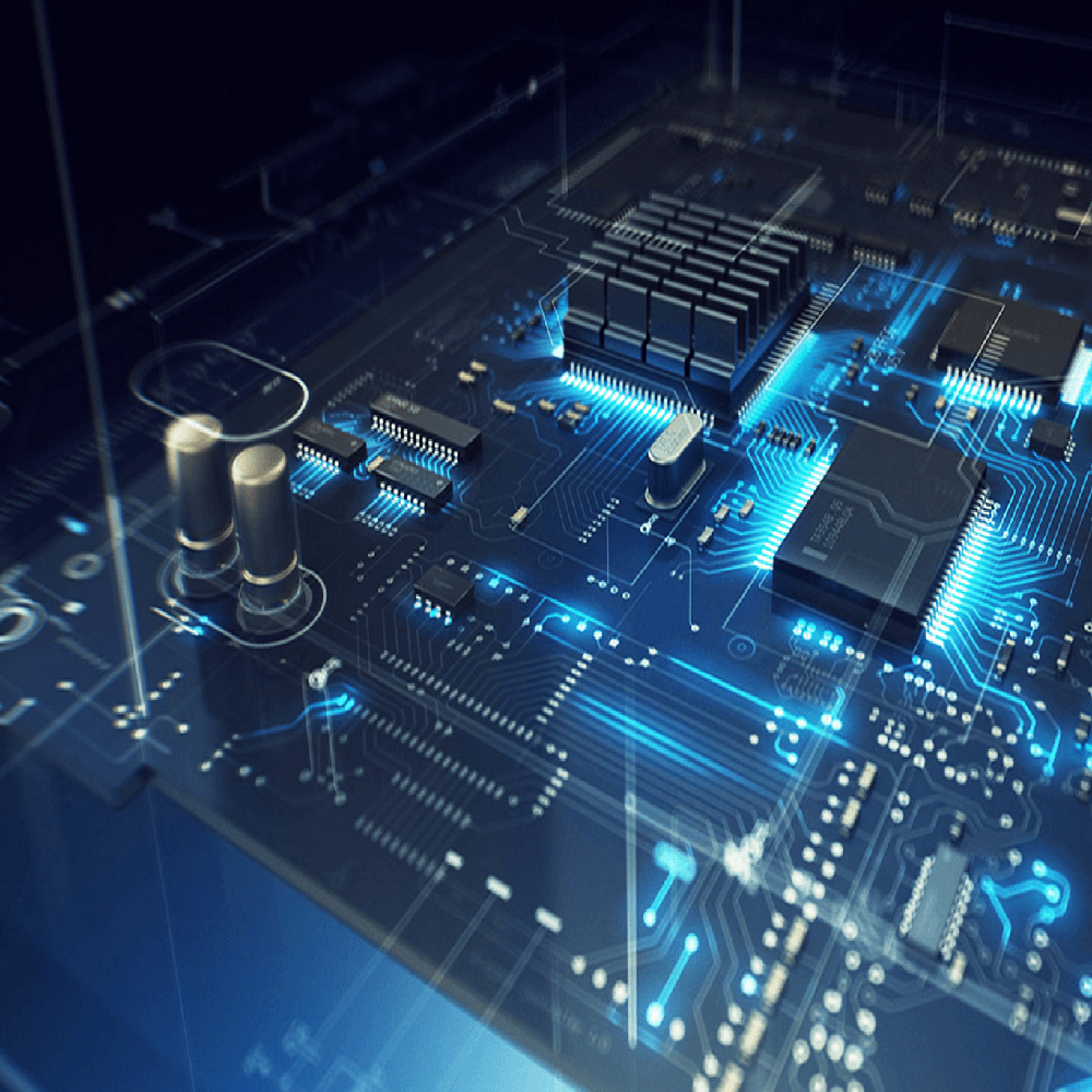
Beyond PCB design, HBeonLabs offers fullproject developmentsupport, includingmicrocontroller programming,firmware development,power supply design,sensor integration,wireless communication (LoRa, GSM, Wi-Fi, BLE), andmechanical enclosure design. Our team takes care ofcomponent sourcing,prototype fabrication,assembly, andfunctional testing, ensuring that every project meets performance, quality, and cost benchmarks.
We specialize in deliveringend-to-end solutionsfor applications such as:
-
IoT-based monitoring and control systems
-
Industrial automation and process control
-
Solar pump controllers and smart energy devices
-
RFID-based access and attendance systems
-
Smart agriculture, healthcare, and wearable electronics
With rapid prototyping capabilities and an agile development approach, HBeonLabs Technologies helps reduce time-to-market and technical risk making us a trusted partner forinnovation, product engineering, and scalable electronics development.
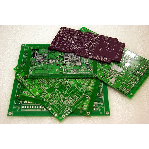
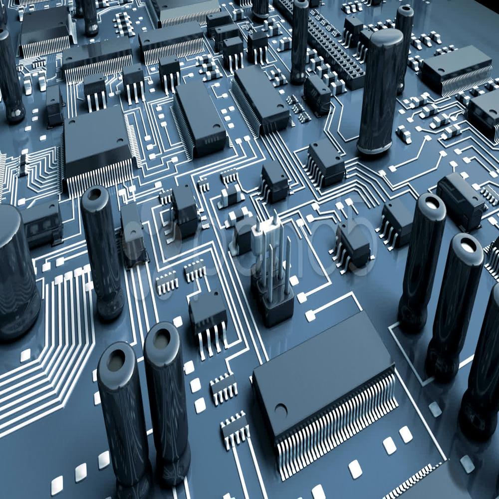
Versatile PCB ManufacturingWhether you need single-layer prototypes or complex multi-layer productions, our facility can accommodate boards up to 500 mm x 600 mm, offering both surface mount and through-hole assembly. We also provide flexible options for copper thickness and PCB materials including FR4, CEM1, and aluminum, making us a one-stop destination for diverse electronic requirements.
Certified Quality and Fast TurnaroundsWith ISO 9001 and UL certifications, alongside full RoHS compliance, quality is assured every step of the process. Automated Optical Inspection and Flying Probe Testing reinforce reliability. Quick lead times mean prototype PCBs can be ready in as little as two days, with production runs fulfilled within 7 to 15 days.
Compatible and Customizable SolutionsWe accept Gerber RS-274X, ODB++, and DXF files from popular design software such as Eagle, Altium, KiCAD, and OrCAD. Choose from various silkscreen and solder mask colors, surface finishes like HASL or ENIG, and board thicknesses ranging from 0.6 mm to 3.2 mm. Our assembly services are matched to both small and large batch requirements.
FAQs of PCB design and making facility:
Q: How do I submit my PCB design files for fabrication?
A: You can submit your PCB design in Gerber RS-274X, ODB++, or DXF formats. Our facility is compatible with Eagle, Altium, KiCAD, and OrCAD outputs. Simply upload your files through our secure portal or email them to our technical team for review before production.
Q: What is the process and turnaround time for prototyping and production?
A: Our prototyping service has a lead time of 2-5 days, while full production orders are completed within 7-15 days. Once your design files are approved, we handle all stepsfrom fabrication of your chosen material and finish to inspection, assembly, and delivery.
Q: Where is your PCB manufacturing facility located and do you serve all of India?
A: Our PCB design and manufacturing facility operates in India, serving customers nationwide. We cater to electronic manufacturers, design houses, and individual developers across the country, ensuring prompt shipment and after-sales support.
Q: What is the benefit of your facilitys quality certifications and testing methods?
A: Our ISO 9001 and UL certifications guarantee adherence to international standards. We employ Automated Optical Inspection (AOI) and Flying Probe Testing at each stage of production, minimizing defects and ensuring reliable, high-quality PCBs every time.
Q: What materials and finishes can I choose for my PCBs?
A: We offer a selection of materials including FR4, CEM1, and aluminum, with customizable board thickness ranging from 0.6 mm to 3.2 mm. Available finishes include HASL, ENIG, OSP, and Immersion Silver, as well as a variety of solder mask and silkscreen colors upon request.
Q: What applications and technologies does your facility support?
A: Our facility supports applications in consumer electronics, industrial automation, automotive electronics, and more. We utilize Surface Mount Technology (SMT) and Through-Hole Technology (THT), accommodating both rapid prototyping and mass production of single to multi-layer PCBs.
Q: How does using your assembly service add value for customers?
A: Our comprehensive assembly services save customers time and resources, enabling quick transition from board fabrication to component assembly. We support both SMT and THT processes, helping streamline your production workflow and reducing overall project timelines.


 Send Inquiry