About Project Based Pcb Design Service
HBeonLabs Technologies offers comprehensive PCB Design and Project Development Services, providing complete electronic product development solutions from initial concept to a fully functional, production-ready prototype. With deep expertise in embedded systems, power electronics, IoT, and automation, we help startups, enterprises, and innovators turn ideas into real, manufacturable hardware products.
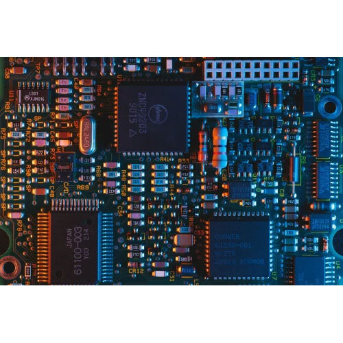
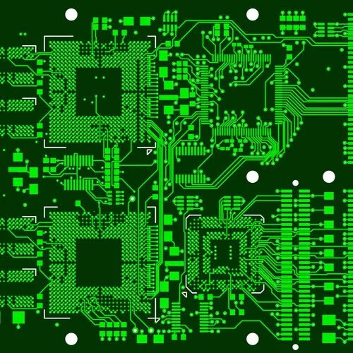
Our PCB design services begin with detailed schematic capture, followed by multi-layer PCB layout using industry-standard tools such as Altium Designer, KiCad, Eagle, and OrCAD. We optimize every design for signal integrity, thermal efficiency, EMI/EMC compliance, and Design for Manufacturability (DFM). Whether its a compact IoT sensor node, a complex industrial controller, or a high-frequency RF board, we tailor the design to your exact requirements.
Beyond PCB design, HBeonLabs offers full project development support, including microcontroller programming, firmware development, power supply design, sensor integration, wireless communication (LoRa, GSM, Wi-Fi, BLE), and mechanical enclosure design. Our team takes care of component sourcing, prototype fabrication, assembly, and functional testing, ensuring that every project meets performance, quality, and cost benchmarks.
We specialize in delivering end-to-end solutions for applications such as:
-
IoT-based monitoring and control systems
-
Industrial automation and process control
-
Solar pump controllers and smart energy devices
-
RFID-based access and attendance systems
-
Smart agriculture, healthcare, and wearable electronics
With rapid prototyping capabilities and an agile development approach, HBeonLabs Technologies helps reduce time-to-market and technical risk making us a trusted partner for innovation, product engineering, and scalable electronics development.
Custom PCB Designs for Every ApplicationWe understand that every project demands unique PCB solutions. Our service supports a versatile range of applications, such as research, industrial prototyping, and educational projects. Through precise manual or automated component placement and in-depth signal integrity analysis, each design is meticulously crafted for optimal function and reliability, regardless of complexity.
Complete Documentation and Quality AssuranceClients receive comprehensive documentation for every project, including Gerber files, Bill of Materials (BOM), schematic diagrams, and assembly drawings. All designs comply with IPC standards for assured quality and reliability. Our testing protocols include functional simulations and design validations to meet both industry requirements and your specific application needs.
Flexible, Secure, and Supportive ServiceWe offer project-based pricing, with lead times and services negotiated according to your requirements. Our team provides technical support after project completion and ensures full confidentiality through non-disclosure agreements when requested. Service is available both online and on-site, covering pan-India, making it convenient and reliable for projects of any size.
FAQs of Project Based Pcb Design Service:
Q: How does the project-based PCB design process work?
A: Our process begins with understanding your specific requirements, which guides us in selecting the right design software and approach. We then provide you with a customized proposal detailing timelines and deliverables. Design, simulation, testing, and documentation follow, with regular updates, until the project is complete and validated.
Q: What documentation will I receive with my PCB design?
A: You will receive a comprehensive set of documents, including Gerber files, Bill of Materials (BOM), schematic diagrams, and assembly drawings. This ensures you have everything required for manufacturing, assembly, and future modifications.
Q: When can I expect my PCB design to be completed?
A: Lead times are flexible and negotiated based on project complexity and your timeline requirements. We work closely with you from the outset to establish realistic milestones, ensuring timely delivery without compromising quality.
Q: Where is the service available, and does it support online collaboration?
A: Our service is available pan-India and can be accessed both online and offline. We facilitate remote collaboration through digital platforms, allowing seamless communication, design reviews, and document sharing, no matter your location.
Q: What are the benefits of your PCB design service over generic solutions?
A: Our project-based approach enables bespoke solutions, tailored documentation, and compliance with IPC standards. Clients benefit from detailed simulations, flexible component placement, dedicated post-design support, and robust confidentiality through NDAs, ensuring reliable and secure project execution.
Q: How can I ensure the confidentiality of my project information?
A: We offer non-disclosure agreements (NDAs) upon request to guarantee the confidentiality of your intellectual property and project details throughout the design and documentation process.
Q: What kinds of applications and industries is this service suitable for?
A: Our PCB design service is ideal for academic research, commercial product development, industrial prototyping, and electronic device innovation. We support diverse applications, from simple single-layer PCBs to complex multilayer systems, ensuring adaptability for various project scopes.


 Send Inquiry