About PCB Designing Cum Layout Designing Services
HBeonLabs Technologies offers comprehensivePCB Design and Project Development Services, providing complete electronic product development solutions from initial concept to a fully functional, production-ready prototype. With deep expertise in embedded systems, power electronics, IoT, and automation, we help startups, enterprises, and innovators turn ideas into real, manufacturable hardware products.
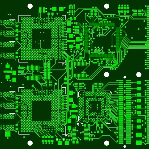
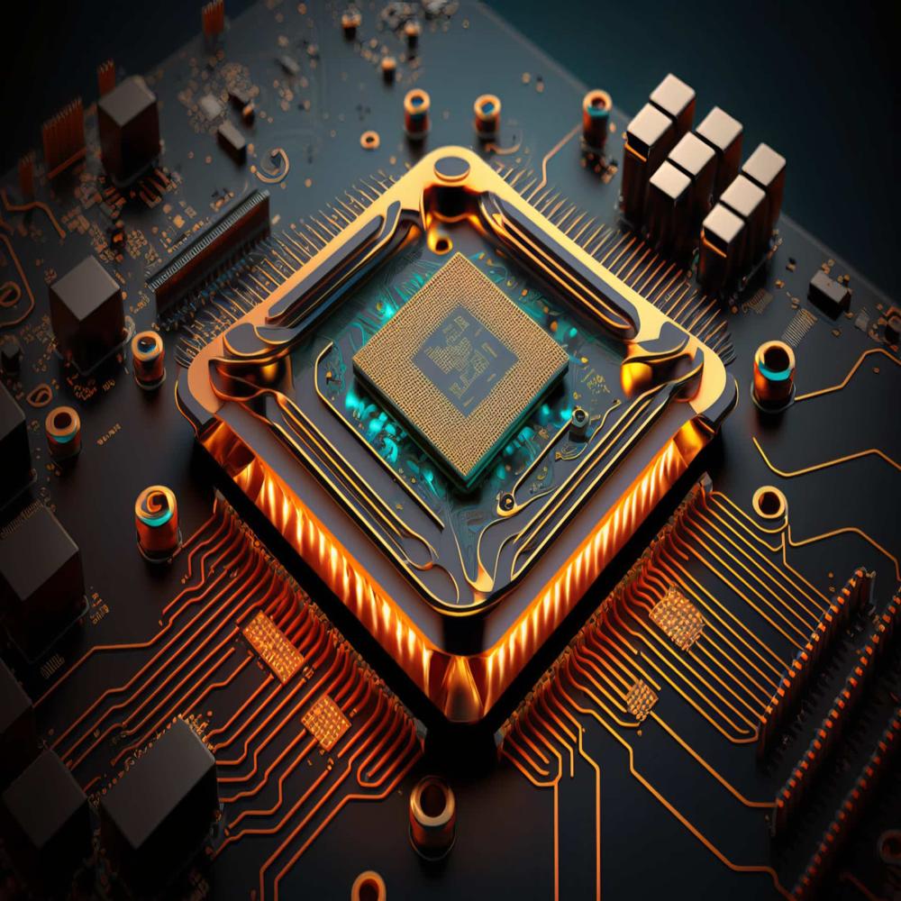
OurPCB design servicesbegin with detailedschematic capture, followed bymulti-layer PCB layoutusing industry-standard tools such asAltium Designer, KiCad, Eagle, andOrCAD. We optimize every design forsignal integrity,thermal efficiency,EMI/EMC compliance, andDesign for Manufacturability (DFM). Whether it's a compact IoT sensor node, a complex industrial controller, or a high-frequency RF board, we tailor the design to your exact requirements.
Beyond PCB design, HBeonLabs offers fullproject developmentsupport, includingmicrocontroller programming,firmware development,power supply design,sensor integration,wireless communication (LoRa, GSM, Wi-Fi, BLE), andmechanical enclosure design. Our team takes care ofcomponent sourcing,prototype fabrication,assembly, andfunctional testing, ensuring that every project meets performance, quality, and cost benchmarks.
We specialize in deliveringend-to-end solutionsfor applications such as:
-
IoT-based monitoring and control systems
-
Industrial automation and process control
-
Solar pump controllers and smart energy devices
-
RFID-based access and attendance systems
-
Smart agriculture, healthcare, and wearable electronics
With rapid prototyping capabilities and an agile development approach, HBeonLabs Technologies helps reduce time-to-market and technical risk making us a trusted partner forinnovation, product engineering, and scalable electronics development.
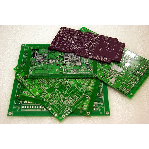
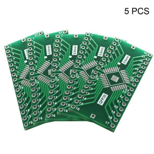
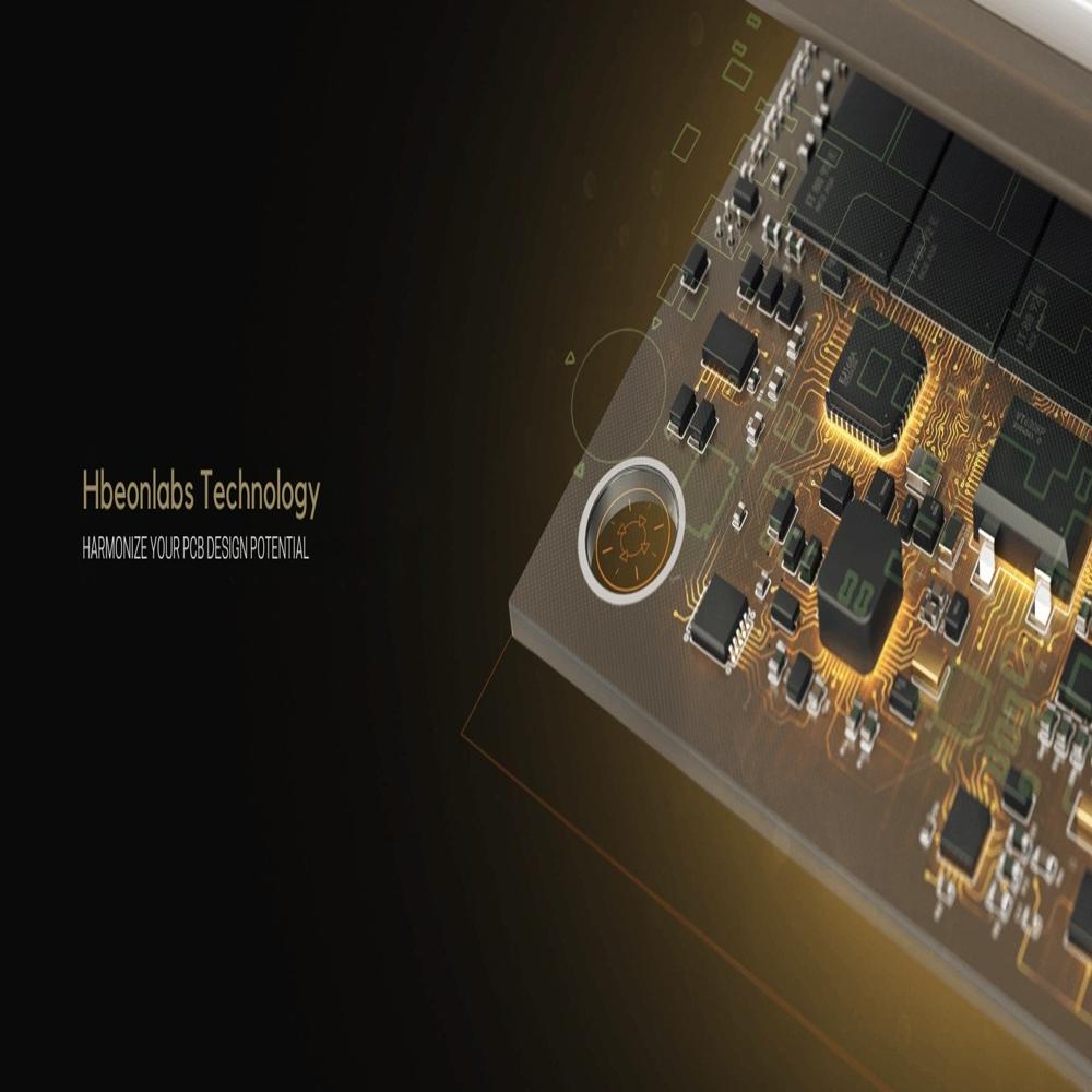
Comprehensive PCB Design SolutionsWe specialize in offering end-to-end PCB designing and layout services for various industries and applications. Whether you require a simple single-layer board or a complex multi-layer solution, our team has the expertise and tools necessary to meet your project specifications and timelines. All services are tailored to client requirements, ensuring reliable results every time.
Advanced Software and Versatile DeliverablesUtilizing industry-standard software such as Altium, Eagle, OrCAD, KiCad, and Proteus, we provide deliverables in formats like Gerber, DXF, PDF, and ODB++. Each project includes a Bill of Materials (BOM), assembly drawings, and comprehensive test support. Our flexible approach means you receive fully customized documentation and layouts, ready for fabrication and assembly.
Nationwide Service with Flexible ModesOperating all over India, we make our PCB design services accessible both online and offline. Our streamlined processes and experienced engineers ensure fast turnaround times-projects are typically completed within 1 to 30 days. No matter your location or project complexity, expect timely, professional, and detail-oriented service every step of the way.
FAQ's of PCB Designing Cum Layout Designing Services:
Q: How is the PCB designing and layout process carried out?
A: The PCB design process begins with schematic entry based on your requirements, followed by layout creation using software like Altium, Eagle, OrCAD, KiCad, or Proteus. Component placement is optimized for both through-hole and surface mount technology. We conduct design rule checks, generate necessary files (Gerber, BOM, etc.), and provide test support for validation before final delivery.
Q: What types of projects and industries can utilize your PCB designing services?
A: Our services are ideal for industrial, research, and commercial projects. From small-scale prototypes to large-volume manufacturing, we support varied applications, including automation, instrumentation, consumer electronics, and academic research, offering scalable solutions to clients across India.
Q: When can I expect the completed PCB design and deliverables?
A: Service duration ranges from 1 to 30 days, depending on the complexity and number of layers in your project. Clear timelines are discussed at the project initiation, and we ensure prompt delivery of all files and documentation within the agreed schedule.
Q: Where are your PCB designing services available?
A: We offer our PCB designing and layout services throughout India, supporting clients both remotely via online channels and in-person through offline modes, according to your location and preference.
Q: What deliverables will I receive at the end of the design process?
A: You will receive comprehensive output including Gerber files, Bill of Materials (BOM), assembly drawings, and component placement files. Supported formats are Gerber, DXF, PDF, and ODB++. The deliverables are fully customized based on your project needs for smooth fabrication and assembly.
Q: How does customization work for PCB layout and deliverables?
A: We adapt our design approach to meet your specifications, whether it's particular layer counts, component types, or preferred file formats. Clients can communicate their requirements during project discussions to ensure the final board layout and documentation align with their goals.
Q: What are the main benefits of choosing your PCB designing services?
A: Clients benefit from our technical expertise, multi-layer support, software versatility, comprehensive deliverables, and robust testing support. Our flexible, client-focused approach and nationwide reach ensure high-quality PCB solutions tailored for industrial, research, or commercial applications.


 Send Inquiry