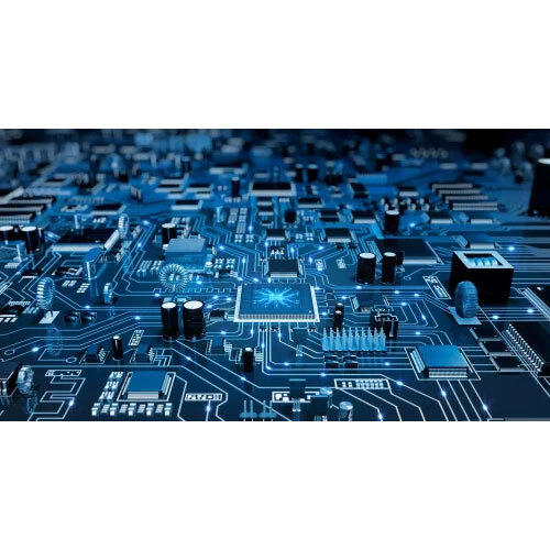
About Computer PCB Design Services
We are a well established manufacturer of Computer PCB Design Services in the market. It is printed circuit board which is made to electrically connect the electronic components through conductive tracks and pads. Computer PCB Design Services form the backbone of all electronic design services. We strive to deliver this on time.
Technical Specification
| Brand | HBeonLabs |
| Service Duration | 1-3 Days |
| Service Location | Greater Noida |
| Service Mlode | Offline |
| Course Location | Pan India |
| Type Of Technology | CAD / CAM |
| Type Of Service Provider | Designing Firm |
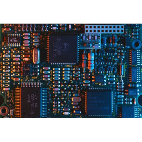
We specialize in PCB design for a variety of computer and electronics hardware applications, utilizing industry-leading tools and standards. From initial concept to final verification, our services cover customized layouts, testing, and component placement, ensuring your project's success. Whether you need a single prototype or a multi-layered board, we offer support throughout India, adapting to your unique requirements.
Precision and Compliance at Every StepEvery PCB is meticulously designed for high accuracy and reliability. Our methodology adheres strictly to IPC standards and incorporates thorough electrical and functional testing. Supporting comprehensive documentation and standardized processes, we deliver robust solutions that meet both regulatory and practical performance criteria.
FAQ's of Computer PCB Design Services:
Q: How do I begin a Computer PCB Design project with your team?
A: You can start by contacting us online or offline through our Pan India service channels. Share your project requirements and specifications, and our experts will guide you through the initial consultation, design planning, and quotation process.
Q: What kinds of PCB designs can you handle for computer applications?
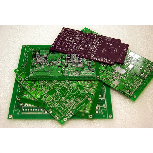
A: We support single, double, and multi-layer PCB designs, tailored for a wide range of electronics and computer hardware. Both SMD and through-hole component placements are available, ensuring compatibility with your product's needs.
Q: When can I expect project completion for PCB design services?
A: The service duration is determined by the complexity and specifics of your project. Upon review of your requirements, we provide an estimated timeline and keep you updated throughout the process.
Q: Where are your PCB design services available across India?
A: Our services are accessible throughout Pan India, allowing clients from any region to utilize our online or offline capabilities for seamless communication and project management.
Q: What is the process involved in PCB design and documentation?
A: After initial consultation, we proceed with schematic creation, layout design using Altium Designer, OrCAD, or Eagle, followed by testing and verification. Documentation-including Gerber files and BOM-is provided as part of project delivery.
Q: How are your PCB design services beneficial for computer hardware projects?
A: Our customized approach, advanced design tools, and adherence to IPC standards ensure high precision and reliable performance. You benefit from comprehensive project support, robust testing, and detailed documentation, aiding seamless manufacturing and deployment.
Q: Is customization available for specific project needs?
A: Yes, we offer full customization to align with your specific project requirements, including PCB layer configuration, component selection, and specialized design features.


 Send Inquiry