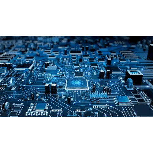
About Pcb Design Service
HBeonLabs Technologies offers comprehensive PCB Design and Project Development Services, providing complete electronic product development solutions from initial concept to a fully functional, production-ready prototype. With deep expertise in embedded systems, power electronics, IoT, and automation, we help startups, enterprises, and innovators turn ideas into real, manufacturable hardware products.
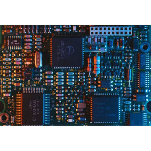
Our PCB design services begin with detailed schematic capture, followed by multi-layer PCB layout using industry-standard tools such as Altium Designer, KiCad, Eagle, and OrCAD. We optimize every design for signal integrity, thermal efficiency, EMI/EMC compliance, and Design for Manufacturability (DFM). Whether its a compact IoT sensor node, a complex industrial controller, or a high-frequency RF board, we tailor the design to your exact requirements.
Beyond PCB design, HBeonLabs offers full project development support, including microcontroller programming, firmware development, power supply design, sensor integration, wireless communication (LoRa, GSM, Wi-Fi, BLE), and mechanical enclosure design. Our team takes care of component sourcing, prototype fabrication, assembly, and functional testing, ensuring that every project meets performance, quality, and cost benchmarks.
We specialize in delivering end-to-end solutions for applications such as:
-
IoT-based monitoring and control systems
-
Industrial automation and process control
-
Solar pump controllers and smart energy devices
-
RFID-based access and attendance systems
-
Smart agriculture, healthcare, and wearable electronics
With rapid prototyping capabilities and an agile development approach, HBeonLabs Technologies helps reduce time-to-market and technical risk making us a trusted partner for innovation, product engineering, and scalable electronics development.
Expertise with Leading PCB Design SoftwareOur team expertly utilizes Altium Designer, Eagle, OrCAD, and KiCAD to deliver precise and reliable PCB layouts tailored to a wide range of applications. With our in-depth knowledge of these platforms, we ensure your projects benefit from state-of-the-art tools that streamline the design process and produce industry-compliant results.
Comprehensive Material and Output OptionsWe support a variety of board materials, including FR-4, CEM-1, Rogers, and flexible PCBs, allowing for custom solutions that match your application needs. Our outputs include Gerber files, BOM, and Pick & Place data, ensuring seamless transition from design to manufacturing and assembly.
All-India Service and Trusted ConfidentialityServing clients across India, we provide offline PCB design services backed by signed NDAs to ensure project confidentiality. Our flexible approach to payment and prototyping support makes collaborating with us secure, convenient, and adaptable to your projects requirements.
FAQs of Pcb Design Service:
Q: How is the PCB design process managed from concept to delivery?
A: Our process begins with a thorough consultation to understand your specifications. We then create the PCB design using your preferred software (Altium Designer, Eagle, OrCAD, or KiCAD) and generate required files such as Gerber, BOM, and Pick & Place. Once approved, we support prototyping, ensuring the design meets compliance standards, and deliver the final output.
Q: What industries can benefit from your PCB design service?
A: We cater to the electronics industry, serving sectors like consumer electronics, industrial automation, medical devices, and more. Our experience and flexibility in design and materials allow us to adapt to diverse application needs.
Q: Where do you provide your PCB design services?
A: Our services are available all over India. No matter your location, you can access our expert offline PCB design solutions and receive prompt, professional support.
Q: What output formats and files will I receive with my PCB design?
A: You will receive industry-standard output files, including Gerber, Bill of Materials (BOM), and Pick & Place files, ensuring a smooth transition from design to manufacturing and assembly.
Q: Which board materials and finishes do you offer?
A: We work with a range of materials including FR-4, CEM-1, Rogers, and flexible PCBs. Surface finishing options include HASL, ENIG, and OSP, selected as per your projects requirements.
Q: When can I expect my PCB design to be completed?
A: Lead time is determined by the complexity of your project. Once we review your requirements, we provide an estimated timeline and keep you informed throughout the design process.
Q: How is confidentiality handled for sensitive projects?
A: We prioritize client confidentiality by offering signed Non-Disclosure Agreements (NDAs). This ensures your proprietary information remains secure during and after the PCB design process.


 Send Inquiry